 |
|||
|
Page Title:
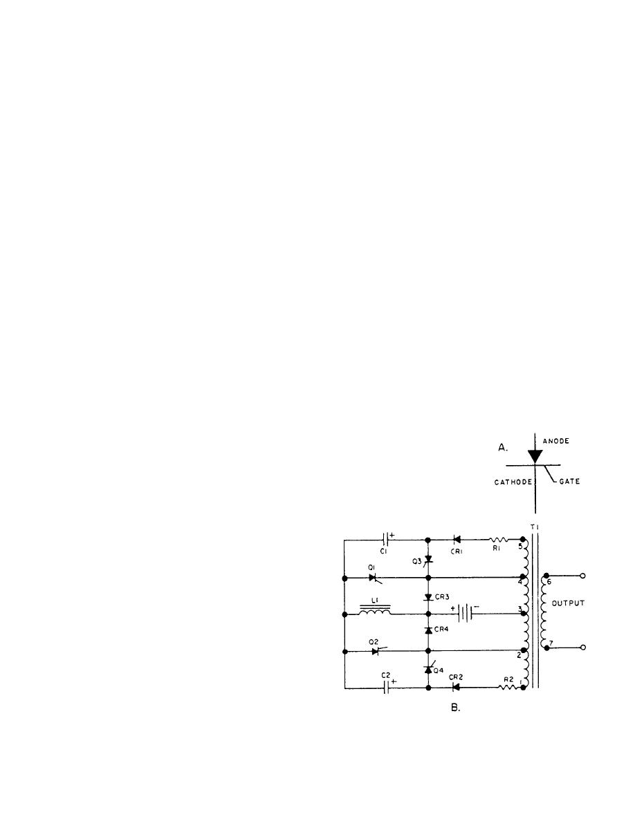
Figure 1-39.-Power stage, simplified schematic diagram. |
|
||
| ||||||||||
|
|
 A unijunction transistor is used to generate the drive
divider (countdown) circuit. The countdown circuit
pulse trigger.
reduces the 1600-Hz oscillator frequency to an 800-Hz
reference frequency required by the inverter control
circuits.
Power Stages
Variable Pulse Width Generators
Each power stage contains three power and three
commutating SCRs for each side of the power stage and
The inverter module contains one variable pulse
a transformer. The SCRs switch the dc source across the
primary of the transformer at a 400-Hz rate to produce
secondary VPWG) (fig. 1-38) and one VPWG for
a 400-Hz square-wave output. The square-wave output
controlling the phase angle between the inverters. Each
is filtered to produce a sine wave.
VPWG contains a monostable (one-shot) multi vibrator,
a modulator circuit, and an inverter output voltage error-
The SCR is the semiconductor equivalent of the gas
sensing circuit.
thyratron tube. Once it is made to conduct, it will
continue to conduct for the remaining positive half cycle
The modulator circuit consists of a transistor and
(anode positive with respect to cathode). Neither the
resistors connected in the discharge path of a capacitor.
removal of the gate voltage nor the reversal of the gate
Varying the level of conduction of the transistor varies
voltage will stop the SCR from conducting. Conduction
the discharge time of the capacitor, which varies the time
may be stopped only by removing the positive anode to
the monostable multivibrator remains in the unstable
negative cathode voltage completely or by applying a
state. The time the monostable multivibrator remains in
slightly greater reverse negative anode to positive
the unstable state determines the width of the output
cathode voltage.
pulse.
The principle of operation of the power stages is
The monostable multivibrator used in the VPWG
illustrated in the simplified schematic diagram in fig-
can be triggered only on positive pulses.
ure 1-39.
The output voltage error-sensing circuit for each
When the power SCR (Q1) is triggered on by an
VPWG receives an ac signal (via the feedback loop)
output pulse from the driver, a rising current will flow
proportional to the output voltage of the inverter. The ac
signal is converted into a corresponding dc signal, com-
pared with a reference signal, and the error (difference)
signal is used to control the level of conduction of the
transistor in the modulating circuit.
The secondary VPWG regulates the output voltage
of phase AB and the phase control, and the main VPWG
regulates the voltages of phases BC and CA. The phase
control VPWG also provides a delay in time between
triggering of the main and secondary VPWG to control
the phase angle between the power stages ( 1 and 2) of
the inverters.
The main and secondary VPWGs deliver one
NM-Hz input to each of the driver stages ( 1 and 2) and
another 800-Hz input to a binary countdown circuit that,
in turn, delivers two 400-Hz inputs 180 apart to each
of the driver stages.
Drivers
Each driver contains four drive pulse generators.
Two of the drive pulse generators generate the triggers
for the power SCRs ("turn on" SCRs), and the other two
generate the triggers for the commutating SCRs ("turn
Figure 1-39.-Power stage, simplified schematic diagram.
off SCRs) in the power stages.
1-32
|
|
Privacy Statement - Press Release - Copyright Information. - Contact Us |
