 |
|||
|
Page Title:
Figure 1-48.--Frequency discriminator, simplified schematic. |
|
||
| ||||||||||
|
|
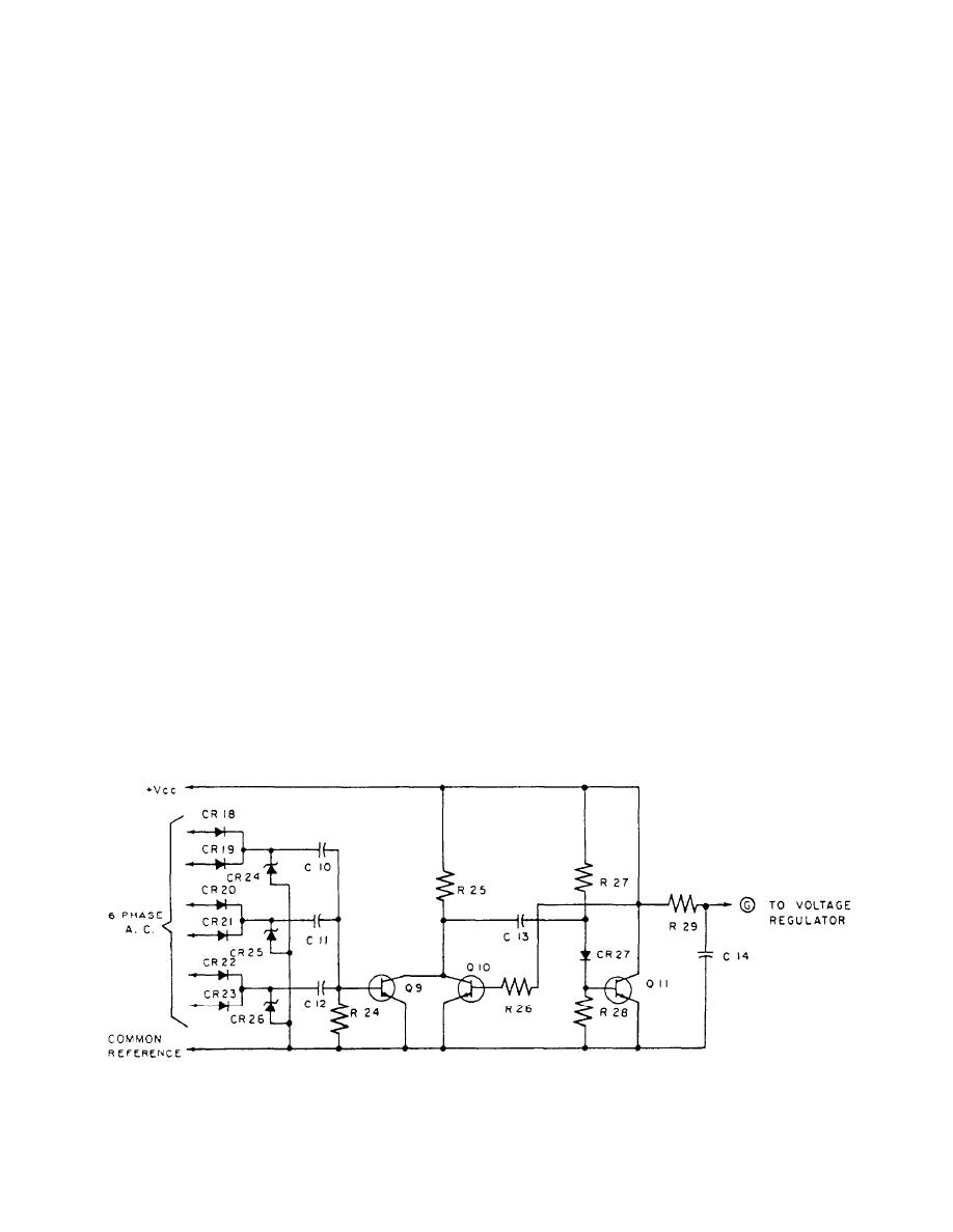 Before the trigger pulse is applied, C13 has been
a decrease in generator field current; but, in the
charged to the collector voltage (Vcc) level through
frequency regulator, an increase infrequency causes the
resistor R25 with the other end clamped to ground
field current to increase.
through diode CR27 and the base-emitter junction of
The discriminator circuit is shown in figure 1-48. It
Q11. When C13 discharges due to the trigger pulse, it
essentially consists of a one-shot multivibrator that puts
turns Q11 off. The collector will rise to the collector
out a constant width pulse whenever a trigger pulse is
voltage level, and resistor R26 will apply base current
applied. The trigger circuitry is designed so a pulse is
to Q10 to hold it saturated after the trigger pulse ends.
applied six times each output cycle to obtain a high
This state (Q10 on, Q11 off) will exist until C13
enough sampling rate to decrease the response time of
charges through R27 to a voltage high enough to allow
the circuit. The multivibrator output is integrated to
Q11 to become forward biased again. At this time the
provide a dc voltage that is proportional and linear with
output pulse ends since Q11 saturates and the base drive
frequency.
of Q10 is removed. The time duration of the output pulse
is controlled by C13 and R27 with CR27 in the circuit
The positive collector voltage input furnishes the
to protect the base junction of Q11 from overvoltage.
circuitry operating biases and 6-phase ac is used to
obtain the trigger pulses. The trigger circuitry consists
The output pulse from the collector of Q11 is fed
through resistor R29 to integrating capacitor C14.
of three single-phase full-wave rectifiers (CR18 and
During the time no output pulse is present, C14 is
CR19, CR20 and CR21, and CR22 and CR21). Each is
discharged through R29 and the collector-emitter
driven from a winding of the T1 star secondary (fig.
junction of Q11.
1-44). The rectified voltages are clipped by the Zeners
(CR24, CR25, and CR26) to obtain a square pulse,
which is further shaped by the differentiating circuitry
of charge time to discharge time increases, which in turn
increases the discriminator output voltage proportional
of C10, C11, C12, and R24. The differentiated pulses
to the frequency shift. A decrease in frequency does the
drive the trigger transistor Q9, which saturates when-
opposite. The output is applied to the error voltage
ever a positive pulse is applied.
detector circuit (base of Q1, fig. 1-44) or its equivalent
Transistors Q10 and Q11 form a one-shot multi-
in the frequency regulator.
vibrator with an output that is a 2-millisecond wide pulse
equal in amplitude to the collector voltage. Q11 is
MAINTENANCE
normally held on through R25, CR27, and R28. Thus,
Q10 is held off as its base drive comes from the collector
Under normal conditions, the motor-generator set
of Q11. Since Q9 saturates when a trigger pulse is
and control equipment require inspection and cleaning
applied, the collector voltage of Q10 is at ground
as designated by the PMS maintenance requirement
cards. When you inspect the motor generator, observe
potential whenever a pulse is applied.
Figure 1-48.--Frequency discriminator, simplified schematic.
1-44
|
|
Privacy Statement - Press Release - Copyright Information. - Contact Us |
